My Digital Systems II class at RIT consisted of 13 lab assignments building one on top of the last. Starting from a simple FPGA demo in lab 1, we then implemented low level logic gates and CL systems to create an Arithmetic Logic Unit in lab 6, this ALU was then integrated into a RISC processor in labs 9 and 10, followed by the design and implementation of a Sequential Shift Right Multipler and Pipelined Shift Right Multipler in labs 11 and 12, with the final project in lab 13 being the integration of the SSRM and PSRM into Simple Neural Networks for recognizing +-/* characters from an image and a full resource/timing analysis of the two Multiplier designs from labs 11 and 12 along with a multipler program than ran on the RISC processor from lab 10. The SSRM is written in VHDL and the RISC and PSRM are written in Verilog. HDL code for all three projects are on my github
The first 10 labs from this course resulted in a RISC processor with 16 instructions that could take two four bit operands (inputted via the dip switches or read from memory) and perform the requested instruction on them. Several specifications came from my Individual Design Number (19) which was used to randomly assign things like memory mapping (Separate Mapped) and organization (Von Neumann) as well as more mundane things like a restriction to use case statements in place of if/else conditional, which is why my Verilog code looks very questional in some places. Trust me I would love to have used an if/else there but I was not allowed to. The procesor took an instruction word of width 8 bits consisting of a 4-bit instruction and two 2-bit register IDs to select the correct busses and registers, and send the appropriate instructions to the ALU as needed for ADD, SUB, INC, DEC, XOR, AND, OR, CPY, SHRA, SHRL, and RRC operations. The remaining operations LD, ST, JUMP, IN, and OUT used the internal busses to connect the data registers to the appropriate memory and IO registers.
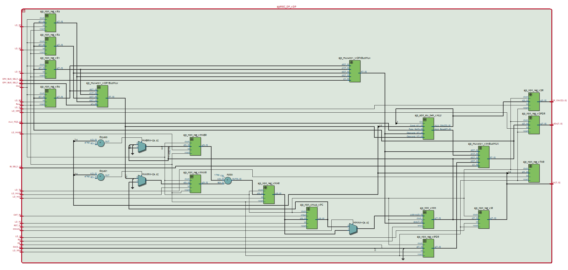
The above image shows the Data Path of the ALU. As needed, the ALU is often fed the most significant 4 bits from the instruction word however in some cases, such as the COPY memory operation, the Transfer Y ALU function is used with the internal busses routed as specified by the least significant 4 bits as this was the simplest way to implement a COPY operation without the need to design another discrete system. The instuctions are processed and routed by the Control Unit which sets appropriate flags during each machine cycle, and the instructions are loaded from lines of machine code stored in a ROM file loaded at system startup which allows the processor to be re-configured for different operations without the need to change any HDL files or re-synthesize the designs.
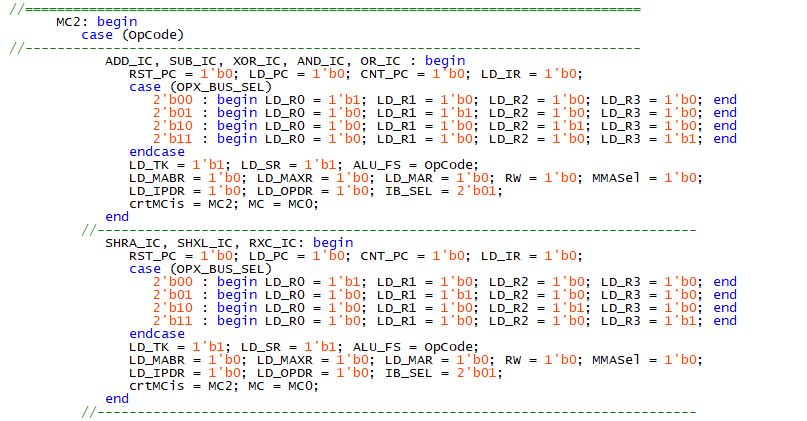
The above image shows a snippet of the RISC Control Unit, with the opcode for arithmetic operations being routed directly to function select of the ALU.
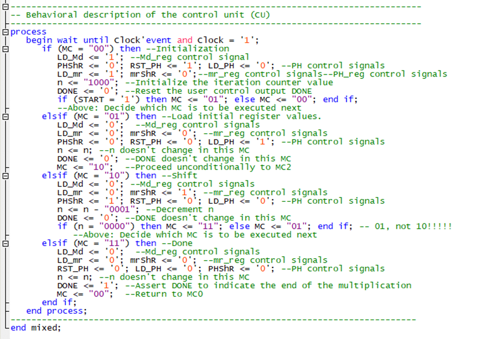
The SSRM and PSRM designs were specified as having an 8-bit multiplier and a 5-bit multiplicand per my Individual Design Number and for the SSRM I elected to implement the design in VHDL. Design and implementation were relatively straight forward with again the split Control Unit/Data Path architecture and the re-use of some combinational logic components from earlier labs. Each multiplcation operation consists of several shift and add operations until the final result is reached and only one multiplcation operation can be processed at a time. The full code for the control unit can be seen in the image below.
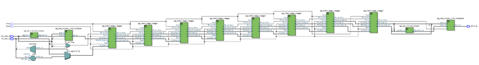
For the PSRM I chose to use Verilog with similar CU/DP split architecture and re-used components however this design implemented the same shift+add algorithm with a much different Data Path. For an 8-bit multiplier, 8 separate stages of shift+add registers were cascaded from one into the next meaning that eight operations could be in-progress at a time and while it would still take eight full cycles to compute any specific output, once the pipeline had been filled a new result could be output on every clock cycle resulting in significant time saved if there are many multiplication operations needing to take place. The Data Path of the PSRM can be seen below, with a majority of logic elements being used to create the eight stages of shift+add registers.
The increased throughput of the PSRM compared to the SSRM became evidently advantageous when implementing each of the multipliers into a Simple Neural Network, as the SSRM necessitated that the neural network run slower than the multipler (~20:1 PSRM clock cycles per SNN clock cycle) when completing those operations while the SSN built on the PSRM could run at a 1:1 time scale with just eight additional clock cycles at the end to clear the pipeline.
Lab 13 focused mostly on performance and timing analysis between the two shift right multipliers and a new multiplier program which was loaded onto the RISC as a ROM, with the design as-is from the end of lab 10. A chart comparing some multiplcation results is shown below
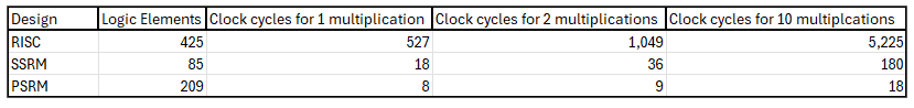
Results were in line with my expectations, in that the physical resource usage of the SSRM is the lowest. The resource usage of the PSRM was marginally higher and had the caveat of always needing to feed dummy values into the multiplier for eight cycles after entering the last set of real values, but was by far the fastest at calculating a single or multiple values and once the pipeline was full a new value could be output on every clock cycle. The multipler program on the RISC unsurprisingly used the most logic elements in its design and took the longest time to calculate the first and every result there-after with the sequential multiplier program loaded; However the flexibility in a general purpose processor design that be re-used in a different application without re-designing the circuit by loading a different program into memory gives a benefit that neither of the other multipliers had in that it could be easily re-configured by someone other than the circuit designer. With no knowledge of the inner-workings of the processor any programmer could read the documentation for the 16 different opcodes and write a new program in the RISC assembly language and compile it into machine code. Time and time again the lesson I have learned from my experience as an engineering student is that engineering is all about optimizing resources to solve a problem, and the time taken to develop a solution is an often overlooked variable in the optimization equation. Developing an efficient pipelined multipler is not the optimal solution if it is only ever going to be used once but there is an inflection point, say in the case of a neural network where there may be thousands or millions of multiplication operations taking place, where is becomes worthwhile to spend more time reducing a few clock cycles from each operation because that equates to millions of clock cycles saved when the operation is done over and over.